

[ad_1]
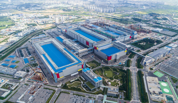
Samsung Electronics will convert a part of its NAND flash manufacturing traces on the Pyeongtaek and Hwaseong campuses into DRAM manufacturing services to reply to the surging semiconductor DRAM demand pushed by the worldwide growth of synthetic intelligence (AI) infrastructure funding. The corporate additionally plans to ascertain Pyeongtaek Plant 4 (P4) as a DRAM-dedicated line making use of the newest course of (1c) to maximise earnings.
An business insider mentioned on Nov. 20, “Samsung Electronics is taking a conservative strategy to the NAND flash market,” including, “Normal-purpose DRAM demand is considerably growing and costs are anticipated to proceed rising, so the corporate is continuing with work to extend manufacturing quantity.”
Reminiscence semiconductors, which help the speedy operations of central processing models (CPUs) and graphics processing models (GPUs), are experiencing shortages as world massive tech corporations are competing to put money into AI infrastructure. Particularly, current market demand for DRAM has been recognized as reaching 3 times the provision capability of the three main reminiscence corporations: Samsung Electronics, SK Hynix, and Micron Know-how. In keeping with business sources, some corporations have supplied to extend costs for Samsung Electronics’ high-capacity server DRAM, together with 96GB and 128GB double information price 5 (DDR5), by 70%, however they’ve been unable to safe volumes as a result of inadequate provide. Main massive tech corporations, anticipating continued DRAM provide shortages, have entered negotiations for provide volumes for 2027.
Samsung Electronics plans to transform a part of its NAND flash manufacturing services into DRAM manufacturing traces to fulfill the surging demand. Presently, the corporate produces DRAM and NAND flash at Pyeongtaek Plant 1 (P1), Plant 3 (P3), and the Hwaseong campus. Pyeongtaek P1 and the Hwaseong campus function as hybrid traces that produce each DRAM and NAND flash. Samsung Electronics will proceed with growth by lowering NAND flash manufacturing services and increasing DRAM manufacturing services at P1 and the Hwaseong campus.
Moreover, P4, which is presently present process ending development, might be accomplished as a 10-nanometer (1 nm = one billionth of a meter) class sixth era (1c) DRAM manufacturing facility and start operations subsequent 12 months. Moreover, the corporate is reviewing a plan to provide DRAM at Plant 2 (P2), which was initially deliberate to deal with foundry (semiconductor contract manufacturing) manufacturing services.
As soon as facility funding is accomplished as early as the primary half of subsequent 12 months, the present hybrid traces at Pyeongtaek P1 and the Hwaseong campus can have a better proportion of DRAM manufacturing, whereas P4 and others will home new DRAM manufacturing traces, considerably growing manufacturing capability. The decreased NAND flash manufacturing quantity domestically is thought to be addressed by growing manufacturing on the Xi’an plant in China. An business official mentioned, “Whereas there are lots of suppliers for NAND flash, the three reminiscence corporations are all the things for DRAM,” including, “Rising manufacturing of extremely worthwhile DRAM creates a construction the place earnings additionally enhance collectively.”
[ad_2]